
Materials Science
AJA ATC-Orion 8 UHV Sputtering Deposition System [TY 121]
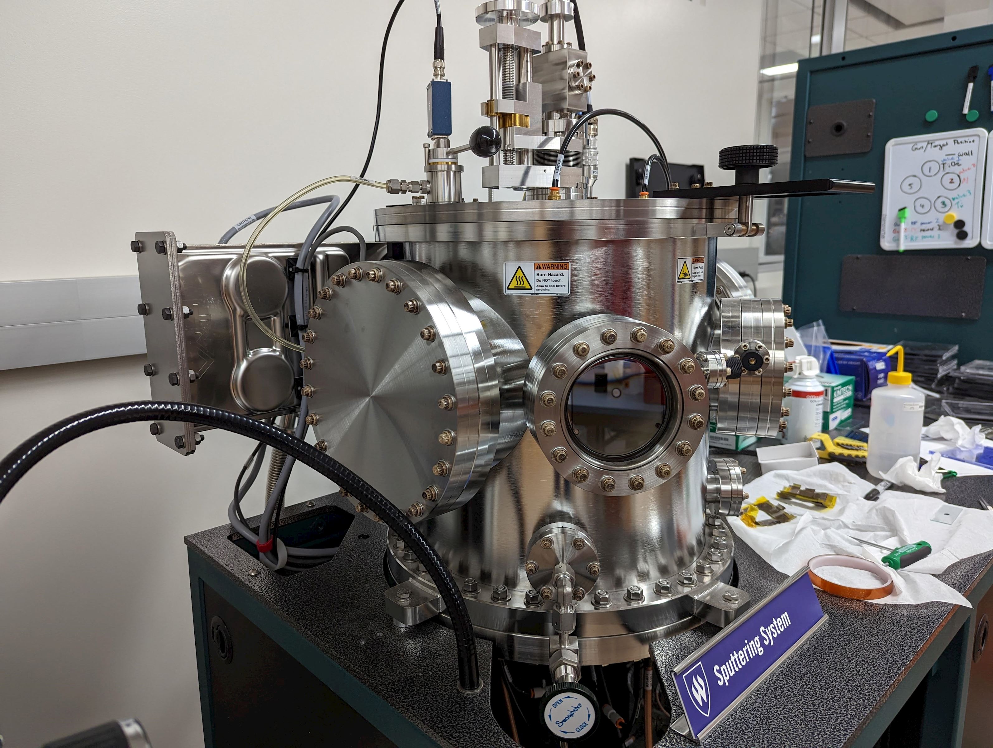
Sputtering systems are used for depositing metal and dielectric thin films on substrates. By depositing different types of materials in specific layers on substrates, various types of thin films can be created, like solar cells or microchips.
This system has a user friendly interface and versatile coating system to allow for a wide range of nanofabrication applications.
Example Use Cases:
- Coat Silicon substrates for production of solar cells
- Confer conductive properties to non-conductive substrates by addition of metal coatings.
Surface Profilometer [TY 121]
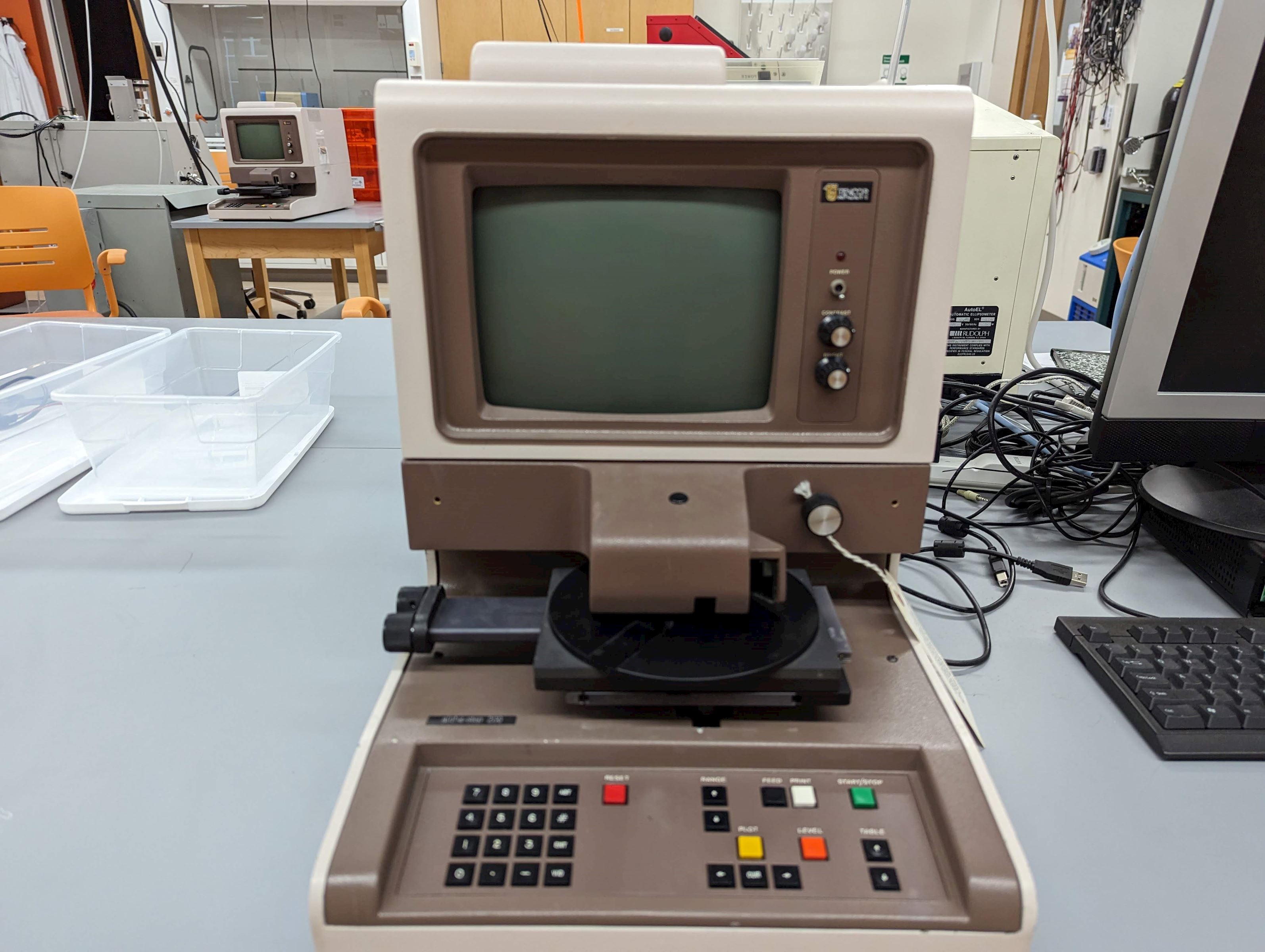
A Surface Profilometer gage is used to capture surface and profile data of a sample in order to measure roughness, flatness, or other critical 2D and 3D dimensions at a very high accuracy.
These measurement principles are regularly used for process control applications where the final product must meet certain specifications for flatness.
Example Use Cases:
- Measure the flatness of coatings applied by the sputtering tool.
- Act as quality control for a production line
Anatech Hummer 6.2 Sputterer and Carbon Coater [TY 121]
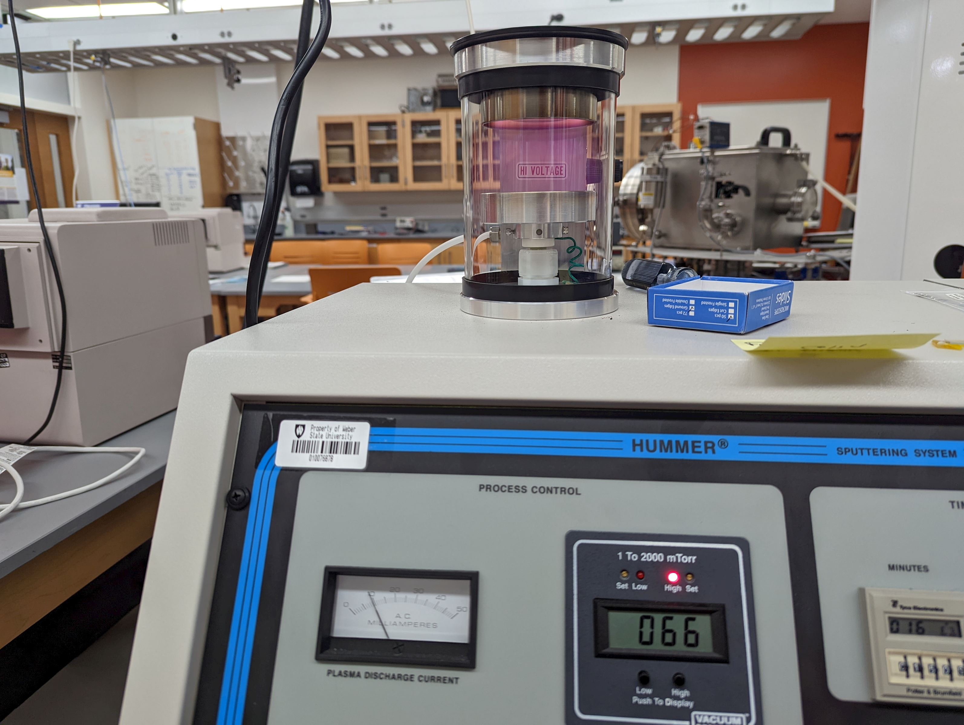
Anatech HUMMER 6.2 performs sputter coating, a cold process in which ions impacting a metal source dislodge metal atoms. The atoms disperse throughout the process chamber to uniformly coat irregularly shaped specimens without thermal damage. Sputter coating produces high quality coatings whose thickness is repeatable and easily controlled.
The Hummer 6.2 also has a Carbon Coating attachment that is useful for coating SEM samples to reduce the amount of charging that occurs due to the electron beam. This can result in much higher quality SEM images for non-metal samples.
Example Use Cases:
- Carbon coat SEM samples to reduce charging effects
- Can coat samples with gold and platinum